

UIG Probe Card Knowledge Popularization | Types and Applications of Probe Cards
Chips that have completed fabrication in wafer fabs but have not yet been packaged are called bare dies, which remain attached to the wafer as individual dies. Since chip packaging incurs high costs and some chip electrical parameters are difficult to test post-packaging, it is critical to conduct performance testing at the bare die stage. This prevents non-conforming (NG) chips from entering the packaging process, thereby reducing overall production costs.
The testing of bare dies prior to packaging is referred to as Wafer Probing or Chip Probing (CP) Testing.

a Wafer Covered with Die
In the CP test process, it is necessary to connect the tester with the chip, and then carry out electrical performance tests. At this time, the external connection ports of the Die are in the form of Pad or Bump. The number of Pads/Bumps on the same Die can be as many as tens of thousands, the size of Pads/Bumps can be as small as dozens of micrometers, and the minimum distance between two adjacent Pads/Bumps can also reach dozens of micrometers. Therefore, connecting the tester with the Die has become a very complex task, and the probe card is the core component to complete this complex task.
The probe card is mainly composed of probes, PCB boards, structural components and electronic components. The needle tip of the probe is used to contact the Pad/Bump on the Die, and the PCB board is used to connect with the tester. In this way, the probe card has become the bridge connecting the Die and the tester.
Due to the different functions, testing requirements, size and shape of chips, as well as the arrangement of Pads/Bumps, the probe card has become a customized product for a specific chip. Moreover, because the probe will wear and consume during continuous use, the probe card itself is also a consumable product.
According to the structure, the mainstream probe cards can be roughly divided into the following three major categories: cantilever probe cards, vertical probe cards and MEMS probe cards. Cantilever probe cards and vertical probe cards have been developed for many years, especially cantilever probe cards, the production technology of many domestic companies has reached a very mature level. However, whether it is a cantilever probe card or a vertical probe card, most of its core components "probes" are purchased from abroad or Taiwan region. Mainland probe card manufacturers mainly undertake the work of design + assembly, and the market share of all mainland probe card manufacturers in the mainland probe card market is very low.

Cantilever Probe Card

Vertical Probe Card
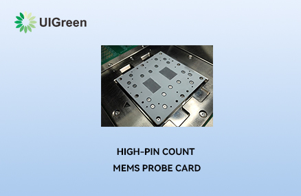
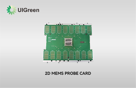
MEMS probe cards, as the most advanced type of probe cards at present, are the best CP test solution at present, and are also the product with the largest market share in the entire probe card market. The manufacturing technology of MEMS probe cards has been monopolized by foreign countries all along. The research in this field in China did not begin to break through until recent years. Our company (UIGreen) has achieved the full-process operations from design to production of 2D MEMS vertical probe cards through investment and research in the field of MEMS probe cards, and it has been delivered to customers for use.
Features of our company’s MEMS probe cards:
• The maximum number of needles on a single needle card is nearly 40,000;
• The minimum test spacing (Pitch) has reached 45 micrometers;
• The maximum current carrying capacity of Diamond MEMS Probe exceeds 2.5A;
• Production experience of True Kelvin CP;
• The three-temperature test can cover -55℃~175℃;
• The test over rejection rate is lower than 1%;
• The life span exceeds 1 million times.


Tel | 0512-87176308
Email | Sales@uigreen.com
Address | 80# Emeishan Road, 196# Putuoshan Road, New District Suzhou,
Jiangsu, China (215163)